- 您现在的位置:买卖IC网 > Sheet目录312 > AT26DF161-SU (Atmel)IC FLASH 16MBIT 66MHZ 8SOIC
�� �
�
�AT26DF161�
�10.1.5�
�10.1.6�
�WEL� Bit�
�RDY/BSY� Bit�
�The� WEL� bit� indicates� the� current� status� of� the� internal� Write� Enable� Latch.� When� the� WEL� bit� is�
�in� the� logical� “0”� state,� the� device� will� not� accept� any� program,� erase,� Protect� Sector,� Unprotect�
�Sector,� or� Write� Status� Register� commands.� The� WEL� bit� defaults� to� the� logical� “0”� state� after� a�
�device� power-up� or� reset.� In� addition,� the� WEL� bit� will� be� reset� to� the� logical� “0”� state� automati-�
�cally� under� the� following� conditions:�
�?� Write� Disable� operation� completes� successfully�
�?� Write� Status� Register� operation� completes� successfully� or� aborts�
�?� Protect� Sector� operation� completes� successfully� or� aborts�
�?� Unprotect� Sector� operation� completes� successfully� or� aborts�
�?� Byte/Page� Program� operation� completes� successfully� or� aborts�
�?� Block� Erase� operation� completes� successfully� or� aborts�
�?� Chip� Erase� operation� completes� successfully� or� aborts�
�If� the� WEL� bit� is� in� the� logical� “1”� state,� it� will� not� be� reset� to� a� logical� “0”� if� an� operation� aborts�
�due� to� an� incomplete� or� unrecognized� opcode� being� clocked� into� the� device� before� the� CS� pin� is�
�deasserted.� In� order� for� the� WEL� bit� to� be� reset� when� an� operation� aborts� prematurely,� the� entire�
�opcode� for� a� program,� erase,� Protect� Sector,� Unprotect� Sector,� or� Write� Status� Register� com-�
�mand� must� have� been� clocked� into� the� device.�
�The� RDY/BSY� bit� is� used� to� determine� whether� or� not� an� internal� operation,� such� as� a� program�
�or� erase,� is� in� progress.� To� poll� the� RDY/BSY� bit� to� detect� the� completion� of� a� program� or� erase�
�cycle,� new� Status� Register� data� must� be� continually� clocked� out� of� the� device� until� the� state� of�
�the� RDY/BSY� bit� changes� from� a� logical� “1”� to� a� logical� “0”.�
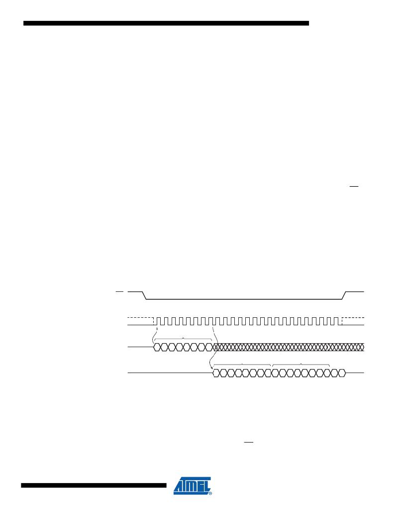
�Figure� 10-1.� Read� Status� Register�
�CS�
�0�
�1�
�2�
�3�
�4�
�5�
�6�
�7�
�8�
�9�
�10� 11� 12� 13� 14� 15� 16� 17� 18� 19� 20� 21� 22� 23� 24�
�SCK�
�OPCODE�
�SI�
�0�
�0�
�0�
�0�
�0�
�1�
�0�
�1�
�MSB�
�STATUS� REGISTER� DATA�
�STATUS� REGISTER� DATA�
�SO�
�HIGH-IMPEDANCE�
�D�
�D�
�D�
�D�
�D�
�D�
�D�
�D�
�D�
�D�
�D�
�D�
�D�
�D�
�D�
�D�
�D�
�D�
�10.2�
�Write� Status� Register�
�MSB�
�MSB�
�MSB�
�The� Write� Status� Register� command� is� used� to� modify� the� SPRL� bit� of� the� Status� Register�
�and/or� to� perform� a� Global� Protect� or� Global� Unprotect� operation.� Before� the� Write� Status� Regis-�
�ter� command� can� be� issued,� the� Write� Enable� command� must� have� been� previously� issued� to�
�set� the� WEL� bit� in� the� Status� Register� to� a� logical� “1”.�
�To� issue� the� Write� Status� Register� command,� the� CS� pin� must� first� be� asserted� and� the� opcode�
�of� 01h� must� be� clocked� into� the� device� followed� by� one� byte� of� data.� The� one� byte� of� data� con-�
�sists� of� the� SPRL� bit� value,� a� don't� care� bit,� four� data� bits� to� denote� whether� a� Global� Protect� or�
�21�
�3599H–DFLASH–8/09�
�发布紧急采购,3分钟左右您将得到回复。
相关PDF资料
AT26DF161A-MU
IC FLASH 16MBIT 70MHZ 8QFN
AT26DF321-SU
IC FLASH 32MBIT 66MHZ 8SOIC
AT27BV010-90JU
IC OTP 1MBIT 90NS 32PLCC
AT27BV020-90JU
IC OTP 2MBIT 90NS 32PLCC
AT27BV040-12JU
IC OTP 4MBIT 120NS 32PLCC
AT27BV1024-90JU
IC OTP 1MBIT 90NS 44PLCC
AT27BV256-70JU
IC OTP 256KBIT 70NS 32PLCC
AT27BV4096-12VI
IC OTP 4MBIT 120NS 40VSOP
相关代理商/技术参数
AT26DF321
制造商:ATMEL 制造商全称:ATMEL Corporation 功能描述:32-megabit 2.7-volt Only Serial Firmware DataFlash Memory
AT26DF321_06
制造商:ATMEL 制造商全称:ATMEL Corporation 功能描述:32-megabit 2.7-volt Only Serial Firmware DataFlash Memory
AT26DF321_07
制造商:ATMEL 制造商全称:ATMEL Corporation 功能描述:32-megabit 2.7-volt Only Serial Firmware DataFlash Memory
AT26DF321-S3U
功能描述:闪存 32M SERIAL FLASH - IND TEMP RoHS:否 制造商:ON Semiconductor 数据总线宽度:1 bit 存储类型:Flash 存储容量:2 MB 结构:256 K x 8 定时类型: 接口类型:SPI 访问时间: 电源电压-最大:3.6 V 电源电压-最小:2.3 V 最大工作电流:15 mA 工作温度:- 40 C to + 85 C 安装风格:SMD/SMT 封装 / 箱体: 封装:Reel
AT26DF321-SU
功能描述:闪存 32M SERIAL FLASH - IND TEMP RoHS:否 制造商:ON Semiconductor 数据总线宽度:1 bit 存储类型:Flash 存储容量:2 MB 结构:256 K x 8 定时类型: 接口类型:SPI 访问时间: 电源电压-最大:3.6 V 电源电压-最小:2.3 V 最大工作电流:15 mA 工作温度:- 40 C to + 85 C 安装风格:SMD/SMT 封装 / 箱体: 封装:Reel
AT26DF321-SU SL514
制造商:Atmel Corporation 功能描述:
AT26F004
制造商:ATMEL 制造商全称:ATMEL Corporation 功能描述:4-megabit 2.7-volt Only Serial Firmware DataFlash Memory
AT26F004_06
制造商:ATMEL 制造商全称:ATMEL Corporation 功能描述:4-megabit 2.7-volt Only Serial Firmware DataFlash Memory